A node claim, and two products to go with it
ChangXin Memory Technologies said on Sunday that its fifth-generation DRAM platform, G5, has entered mass production, and showed two 24-gigabit LPDDR5X parts built on it. The announcement was made at the World Manufacturing Convention in Hefei, in Anhui province, where the company is based.
CXMT put the half-pitch of the active area in the memory array at 11.95 nanometres, reached with quadruple patterning — repeating exposure steps to draw features finer than a single pass can resolve. The company said the platform produces at least 50 per cent more dies per wafer than the previous generation, and called the change a quantum leap in storage density.
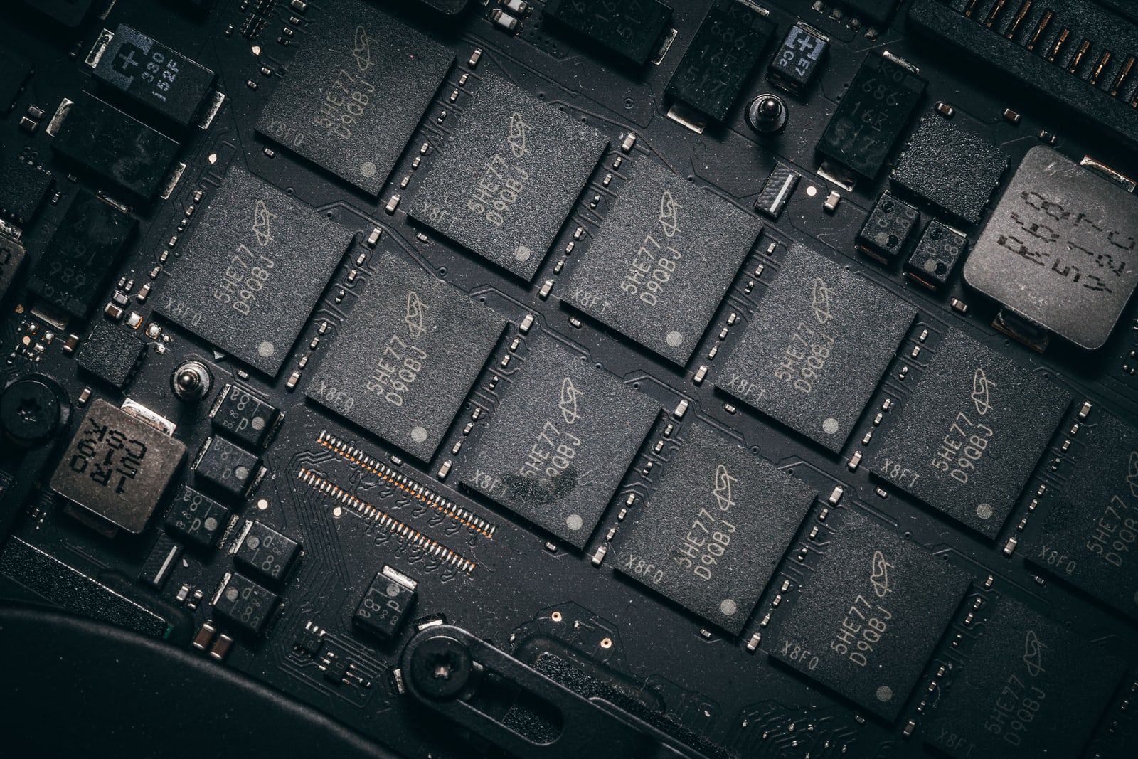
The two LPDDR5X parts hold 3 gigabytes on a single die, half again as much as the 16-gigabit parts that are standard today. Both are in volume production, according to the company, and are used in mainstream Chinese flagship smartphones.
How close is close
Luo Xiaodong, a vice president at CXMT, said the company’s process capability has reached a level on par with the most advanced nodes now in mass production across the industry. Samsung and SK hynix currently ship what they describe as 10-nanometre-class DRAM.
That comparison is looser than it looks. DRAM makers do not use a shared definition of a node, and 11.95 nanometres describes the half-pitch of one structure rather than a whole process. Analysts quoted by the Seoul Economic Daily noted that the figure is not directly comparable with the 12-nanometre-class labels rivals use for their own parts.
The two numbers that would settle it were not given. CXMT disclosed neither yields nor monthly wafer output, so the announcement establishes that the platform runs, not how economically it runs or at what scale.
The market position behind the claim
CXMT held 9.5 per cent of global DRAM revenue in the second quarter of 2026, according to TrendForce, fourth behind Samsung, SK hynix and Micron. That is a substantial move for a company founded in 2016, and it means the three incumbents together now hold a smaller share of the market than they have in over a decade.

Memory is where the export-control regime has bitten least cleanly. Advanced logic fabrication in China remains constrained by equipment restrictions, but DRAM at this class of geometry is reachable with multiple patterning on tools that are already installed — which is precisely what quadruple patterning is for. It costs more steps, and therefore more time and more wafer, than a single exposure on an advanced lithography tool would. It does not require one.
What to watch
The near-term question is whether the G5 parts show up in high-bandwidth memory. HBM stacks are where the money is in AI hardware, and they are built from DRAM dies of roughly this class. CXMT has not announced an HBM product on G5, and moving from mobile LPDDR5X to stacked, through-silicon-via HBM is a different manufacturing problem, not a repackaging exercise.
The second is price. A domestic supplier at 10 per cent share with a denser process is a credible source of pressure on commodity DRAM pricing — which has been running hot on AI demand — in a way a supplier at 1 per cent was not.