A chip for serving models, not training them
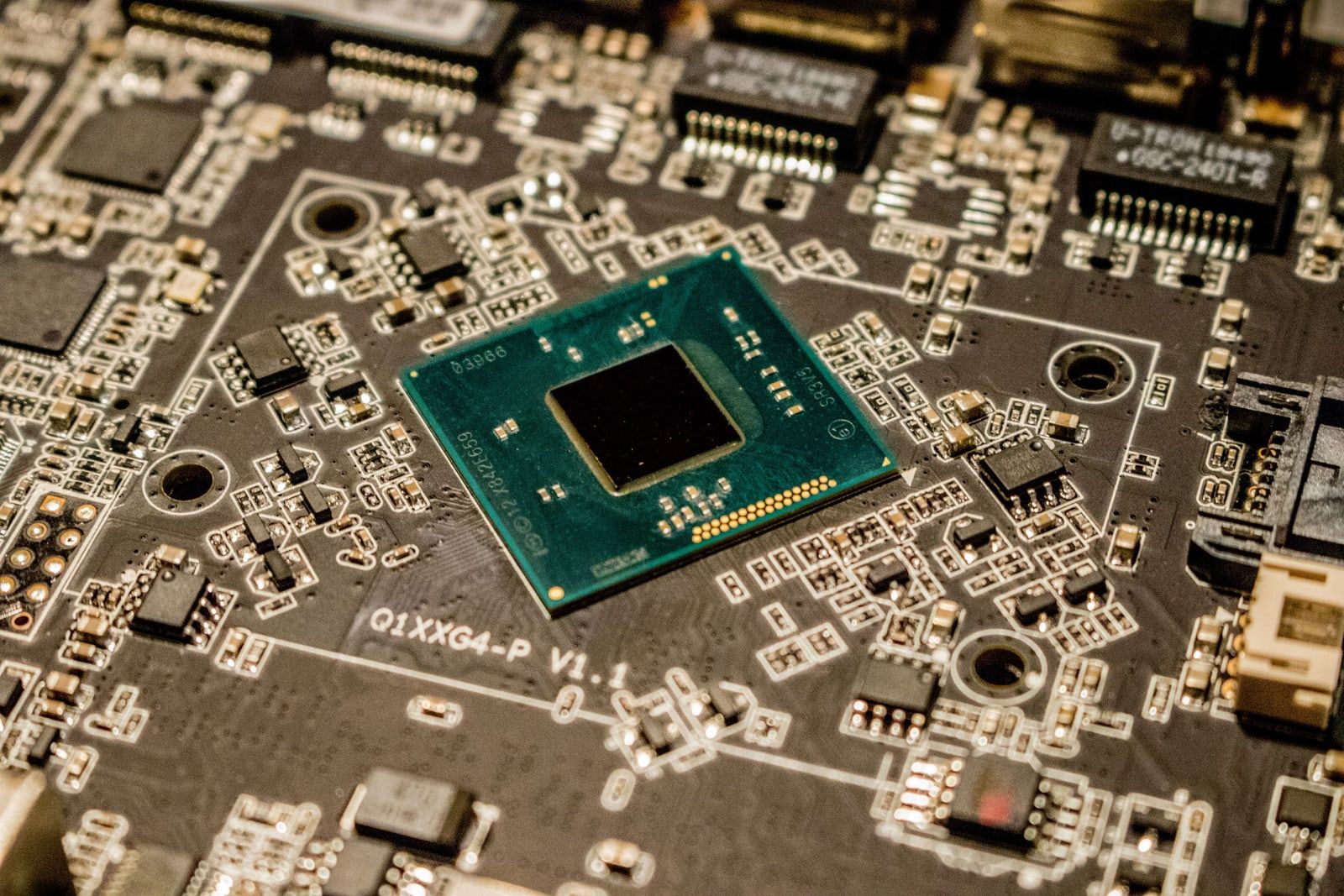
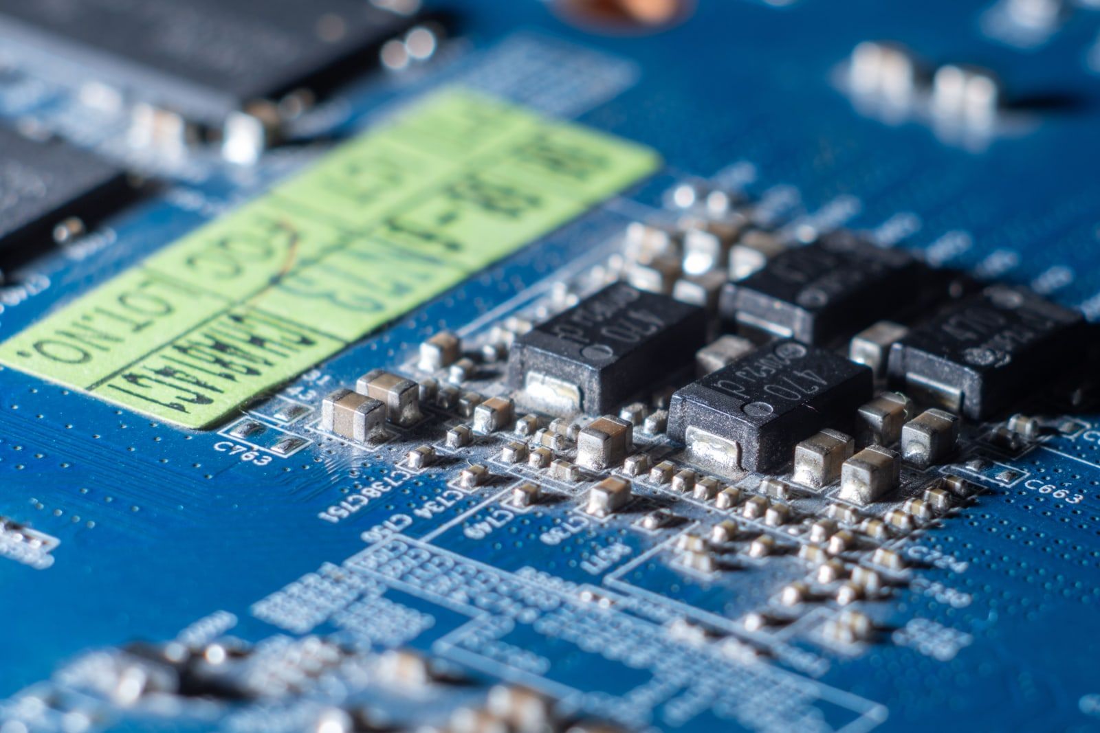
Microsoft published the architecture of Azure Maia 300 on Monday, the third generation of the accelerator it designs for its own data centres. Each chip carries eight stacks of HBM4 memory totalling 288GB with 18TB/s of bandwidth, and its compute chiplets are built on TSMC’s N2P process, with the memory controllers and input-output functions moved onto separate dies.
The design goal, as Azure hardware president Rani Borkar and systems architecture vice-president Saurabh Dighe put it in Microsoft’s own write-up, is to “maximize useful tokens per watt and useful tokens per dollar”. That is a narrower ambition than a general-purpose accelerator sets itself. Maia 300 is built for inference — running models that have already been trained — and Microsoft describes a system tuned end to end for serving large language models rather than for training runs.
Every number is measured against Maia 200
Microsoft’s comparisons are all against Maia 200, the inference part it introduced in January. Against that chip it claims 36% more compute throughput, 2.5 times the memory bandwidth, 33% more memory capacity, roughly twice the bandwidth per watt and 14% more scale-up bandwidth. At rack level it claims up to seven times the token throughput and up to 2.5 times the performance per watt.

These are the vendor’s own figures, set against the vendor’s own previous generation. UPI reported that no third party had tested Maia 300 as of Monday. A separate claim — that the chip will deliver about 40% more tokens per megawatt than leading GPU systems — appeared in reporting on the launch without Microsoft naming the systems it measured against.
The rack is the unit
The more striking part of the disclosure is the enclosure. Microsoft is putting 96 accelerators in a single rack, in 24 trays of four, double the density of Maia 200, and drawing 167kW. Six high-radix switch chips sit in three liquid-cooled switch trays, power arrives on a 50V busbar through dual feeds, and liquid cooling carries away more than 80% of the rack’s heat. Sites without facility water can run the same rack through a heat exchanger.
For comparison, Reuters put Nvidia’s GB300 rack at 72 GPUs and roughly 142kW. Microsoft is asking a rack to swallow more power and more silicon than that, which is the direction the whole industry’s enclosures have been heading.
Above the rack, Microsoft describes a “superpod” of up to 12,288 accelerators spread across as many as 128 racks, with up to 750GB/s available to any peer in the pod depending on where a job lands. It also switched the memory layout across chiplets from uniform to non-uniform access, and added enhanced MXFP4 and sub-3-bit storage formats with conversion handled in hardware — all of which only makes sense if the workload is inference at scale.
What is not in the post
Microsoft gave no deployment dates. The reporting around the launch says the chip goes into production in 2027 and becomes the main system running AI inside Microsoft’s products from that year, with deployments measured in gigawatts. The Information reported in August that Microsoft was in talks with TSMC for more than 300,000 Maia 300 chips for 2027; that remains a report rather than a confirmed order.
Nvidia is not being displaced here. Microsoft’s post is about one part of one workload, and the company continues to buy Nvidia hardware for training. The next concrete marker is Microsoft Ignite, which runs 17–20 November in San Francisco, where Borkar and Dighe say they will say more about how the chip fits the wider strategy.