What the company is
Kepler Computing, based in San Jose and founded in 2018, came out of stealth around 10 September with $468m raised and a memory architecture it says addresses the bottleneck that limits AI inference: getting data in and out of memory fast enough to keep the compute busy.
The investor list is the part that makes the claim worth reading. The company names Addition, Gates Frontier, Temasek, Intel Capital and AMD Ventures among its backers, and says it was selected for up to $245m in proposed US government support, with a Commerce Department announcement in July 2026. Reports put GlobalFoundries in the round too, with a direct investment of $50m.
The technical bet
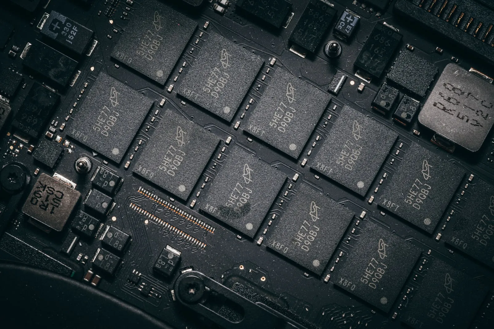
Kepler stacks ferroelectric RAM tiles on top of logic chips. Ferroelectric materials — in this case hafnium-oxide-based — hold their polarisation state without power, and the company says the resulting memory approaches SRAM’s bandwidth per watt while going beyond both SRAM and HBM on capacity. Reports of its claims put that at up to ten times HBM capacity. Those are the company’s figures on its own unshipped product, and no independent measurement exists.
Why the manufacturing story matters more
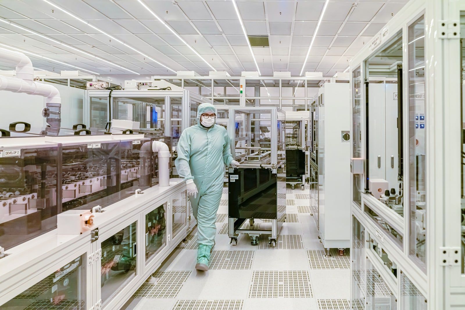
The interesting claim is not the memory. It is the fab. Kepler says it does not need extreme ultraviolet lithography — the tool that gates access to leading-edge nodes and costs hundreds of millions per unit. Instead it layers new materials onto mature 28nm lines, and says it converted a standard 28nm plant into a memory fab in about eight months, against the two years or more a new DRAM facility typically takes.
If that holds, the constraint on AI memory supply stops being EUV capacity and becomes materials engineering on equipment that already exists in quantity. That is a different shape of bottleneck, and a much less concentrated one.
The timeline
The company says it will sample chips in 2026 and reach production in 2027. Reports describe production ramping at a GlobalFoundries facility in Singapore in 2027, with US manufacturing following in 2028. Kepler’s own site also refers to a dedicated 300mm fab and scaling up in America.
What to watch
Two things decide this. Endurance: ferroelectric memory’s historical weakness is fatigue — degradation after repeated polarisation switching — and surviving a lab does not mean surviving a production wafer run at yield. And adoption: memory only matters if accelerator vendors design around it, which means the 2027 date is really a question about whose roadmap has a slot for it.